


Applications
●10GBASE-LR at 10.3125Gbps
●10GBASE-LW at 9.953Gbps
●Other optical link
Product Descriptions
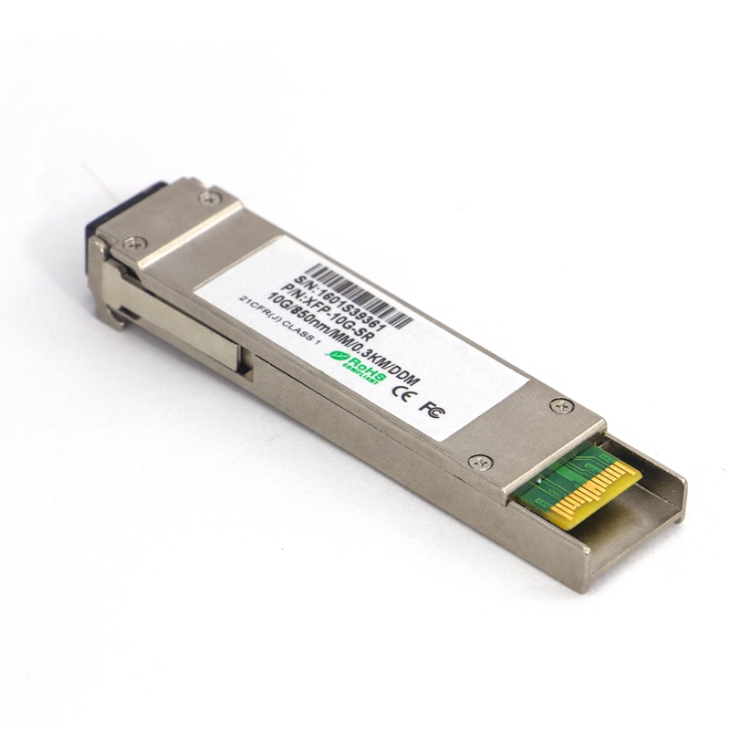
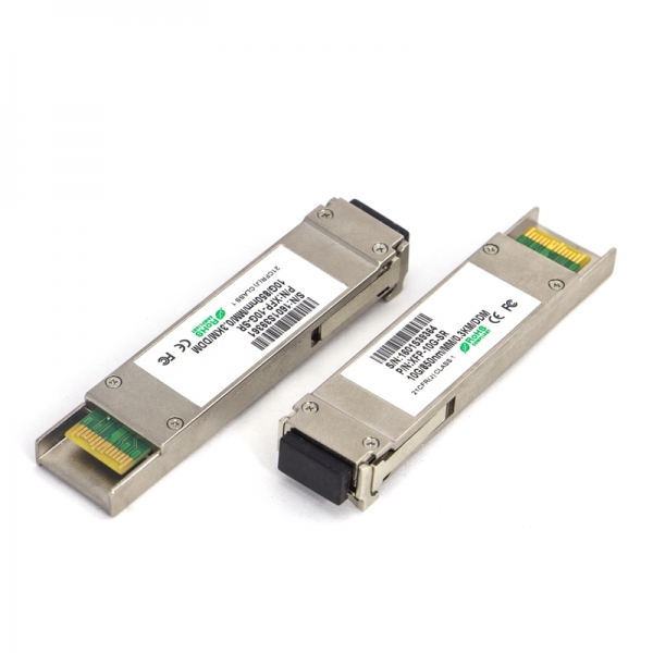
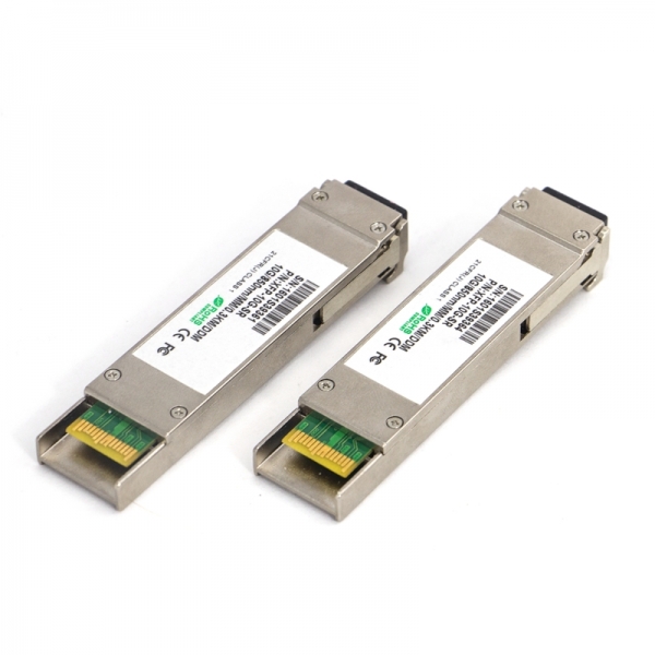
The XFP Bidi is compliant with the IEEE803.3ae 10Gbase-Bx. and transmission distance up to 20km on SMF .The transceiver module comprises a transmitter with a 1270 or 1330nm DFB laser transmitter, an integrated 1330 or 1270nm detector preamplifier(IDP) mounted in an optical header and a limiting post-amplifier IC. Transmitter and receiver are separate within a wide temperature range of 0℃ to +70℃ for commercial temperature, -40 to 80 °C for industrial temperature, and offers optimum heat dissipation and excellent electromagnetic shielding for 10 GbE systems application.
Absolute Maximum Ratings
|
Parameter |
Symbol |
Min. |
Max. |
Unit |
Note |
|
Supply Voltage |
Vcc |
-0.5 |
4.0 |
V |
|
|
Storage Temperature |
TS |
-40 |
85 |
°C |
|
|
Relative Humidity |
RH |
0 |
85 |
% |
|
Note: Stress in excess of the maximum absolute ratings can cause permanent damage to the transceiver.
General Operating Characteristics
|
Parameter |
Symbol |
Min. |
Typ |
Max. |
Unit |
Note |
|
Data Rate |
DR |
9.95 |
10.3125 |
11.3 |
Gb/s |
|
|
Supply Voltage |
Vcc |
3.13 |
3.3 |
3.47 |
V |
|
|
Supply Current |
Icc5 |
|
|
500 |
mA |
|
|
Operating Case Temp. |
Tc |
0 |
|
70 |
°C |
|
|
TI |
-20 |
|
80 |
|
Electrical Characteristics (TOP(C) = 0 to 70 ℃, TOP(I) =-20 to 80 ℃,VCC = 3.13 to 3.47 V)
|
Parameter |
Symbol |
Min. |
Typ |
Max. |
Unit |
Note |
|
Differential data input swing |
VIN,PP |
120 |
|
820 |
mVpp |
|
|
Transmit Disable Voltage |
VD |
2.0 |
|
Vcc |
V |
1 |
|
VEN |
Vee |
|
Vee+0.8 |
|
||
|
Input differential impedance |
Rin |
|
100 |
|
Ω |
2 |
|
Transmit Disable Assert Time |
Tda |
|
|
10 |
us |
|
|
Differential data output swing |
Vout,pp |
340 |
|
850 |
mVpp |
3 |
|
Output rise time and fall time |
Tr, Tf |
|
|
38 |
Ps |
4 |
|
LOS Fault |
VLOS_F |
VCC-0.5 |
|
Vcc |
V |
5 |
|
LOS Normal |
VLOS_N |
Vee |
|
Vee+0.5 |
V |
5 |
Notes:
1. Or open circuit.
2. After internal AC coupling.
3. Into 100 ohms differential termination.
4. 20 – 80 %.
5. Loss Of Signal is open collector to be pulled up with a 4.7k~ 10k resistor to 3.15 – 3.6V.
Logic 0,indicates normal operation; logic 1 indicates no signal detected.
Optical Characteristics (TOP(C) = 0 to 70 ℃, TOP(I) =-20 to 80 ℃,VCC = 3.13 to 3.47 V)
|
Parameter |
Symbol |
Min. |
Typ |
Max. |
Unit |
Note |
|
Transmitter |
||||||
|
Operating Wavelength |
λ |
1260 |
1270 |
1280 |
nm |
|
|
1320 |
1330 |
1340 |
|
|||
|
Ave. output power (Enabled) |
PAVE |
-3 |
|
3 |
dBm |
1 |
|
Side-Mode Suppression Ratio |
SMSR |
30 |
|
|
dB |
|
|
Optical Modulation Amplitude |
POMA |
-2.8 |
|
0 |
dB |
OMA |
|
Extinction Ratio |
ER |
4 |
4.5 |
|
dB |
|
|
RMS spectral width |
Δλ |
|
|
0.45 |
nm |
|
|
Rise/Fall time (20%~80%) |
Tr/Tf |
|
|
45 |
ps |
|
|
Dispersion penalty |
TDP |
|
|
3.2 |
dB |
|
|
Relative Intensity Noise |
RIN |
|
|
-130 |
dB/Hz |
|
|
Output Optical Eye |
Compliant with IEEE 0802.3ae |
|||||
|
Receiver |
||||||
|
Operating Wavelength |
λ |
1320 |
1330 |
1340 |
nm |
|
|
1260 |
1270 |
1280 |
|
|||
|
Receiver Sensitivity(ER=4.5) |
PSEN1 |
|
|
-12.6 |
dBm |
2 |
|
Receiver Sensitivity(ER=6) |
PSEN2 |
|
|
-14.4 |
2 |
|
|
Average Receive Power |
PAVE |
|
|
0.5 |
dBm |
|
|
Receiver Reflectance |
Rrx |
|
|
-12 |
dB |
|
|
LOS Assert |
Pa |
-30 |
|
|
dBm |
|
|
LOS De-assert |
Pd |
|
|
-17 |
dBm |
|
|
LOS Hysteresis |
Pd-Pa |
0.5 |
|
|
dB |
|
Notes:
1. Average power figures are informative only, per IEEE 802.3ae.
2. Measured with worst ER; BER<10-12; 231 – 1 PRBS.
|
PIN # |
Name |
Function |
Name/Description |
Notes |
|
1 |
|
GND |
Module Ground |
1 |
|
2 |
|
VEE5 |
Optional -5.2V Power Supply (Not requireed) |
|
|
3 |
LVTTL-I |
MOD_DESEL |
Module De-select; When held low allows the module to respond to 2-wire serial interface |
|
|
4 |
LVTTL-O |
INTb |
Interrupt; Indicates presence of an important condition which can be read via the 2-wire serial interface |
2 |
|
5 |
LVTTL-I |
TX_DIS |
Transmitter Disable; Turns off transmitter laser output |
|
|
6 |
|
VCC5 |
+5V Power Supply (Not required) |
|
|
7 |
|
GND |
Module Ground |
1 |
|
8 |
|
VCC3 |
+3.3V Power Supply |
|
|
9 |
|
VCC3 |
+3.3V Power Supply |
|
|
10 |
LVTTL-I/O |
SCL |
2-Wire Serial Interface Clock |
2 |
|
11 |
LVTTL-I/O |
SDA |
2-Wire Serial Interface Data Line |
2 |
|
12 |
LVTTL-O |
MOD_Abs |
Indicates Module is not present. Grounded in the Module |
2 |
|
13 |
LVTTL-O |
MOD_NR |
Module Not Ready; Indicating Module Operational Fault |
2 |
|
14 |
LVTTL-O |
RX_LOS |
Receiver Loss Of Signal Indicator |
2 |
|
15 |
|
GND |
Module Ground |
1 |
|
16 |
|
GND |
Module Ground |
1 |
|
17 |
CML-O |
RDN |
Receiver Inverted Data Output |
|
|
18 |
CML-O |
RDP |
Receiver Non-Inverted Data Output |
|
|
19 |
|
GND |
Module Ground |
1 |
|
20 |
|
VCC2 |
+1.8V Power Supply (Not required). |
|
|
21 |
LVTTL-I |
P_DOWN/RST |
Power down; When high, requires the module to limit power consumption to 1.5W or below. 2-Wire serial interface must be functional in the low power mode. |
|
|
21 |
LVTTL-I |
P_DOWN/RST |
Reset; The falling edge initiates a complete reset of the module including the2-wire serial interface, equivalent to a power cycle. |
|
|
22 |
|
VCC2 |
+1.8V Power Supply (Not required) |
|
|
23 |
|
GND |
Module Ground |
1 |
|
24 |
PECL-I |
REFCLK+ |
Not used, internally terminated to 50ohm (100ohm diff). |
3 |
|
25 |
PECL-I |
REFCLK- |
Not used, internally terminated to 50ohm (100ohm diff). |
3 |
|
26 |
|
GND |
Module Ground |
1 |
|
27 |
|
GND |
Module Ground |
1 |
|
28 |
CML-I |
TD- |
Transmitter Inverted Data Input |
|
|
29 |
CML-I |
TD+ |
Transmitter Non-Inverted Data Input |
|
|
30 |
|
GND |
Module Ground |
1 |
Notes:
Notes:
1. Module circuit ground is isolated from module chassis ground within the module.
2. Open collector; should be pulled up with 4.7k – 10k ohms on host board to a voltage between 3.15Vand 3.6V.
3. Reference Clock input is not required.
Management Interface
Typical Interface Ciruit
Ordering Information
|
Description |
|
XFP Bidi,9.95 to 11.3Gb/s, 1270/1330nm, 20km, 0~70℃, with Digital Diagnostic Monitor |
|
XFP Bidi,9.95 to 11.3Gb/s, 1330/1270nm, 20km, 0~70℃, with Digital Diagnostic Monitor |
|
XFP Bidi,9.95 to 11.3Gb/s, 1270/1330nm, 20km, -20~80℃, with Digital Diagnostic Monitor |
|
XFP Bidi,9.95 to 11.3Gb/s, 1330/1270nm, 20km, -20~80℃, with Digital Diagnostic Monitor |


 Josie
Josie  Chat Now
 Josie
Josie  Josie
Josie