


Applications
●10GBASE-LR at 10.3125Gbps
●10GBASE-LW at 9.953Gbps
●Other optical link
Product Descriptions
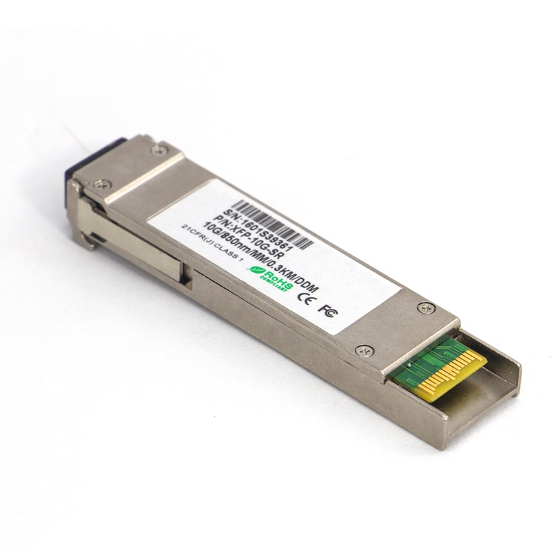
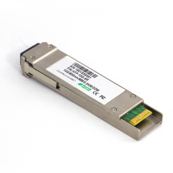
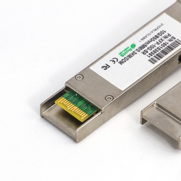
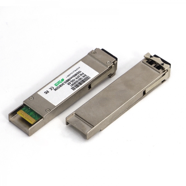
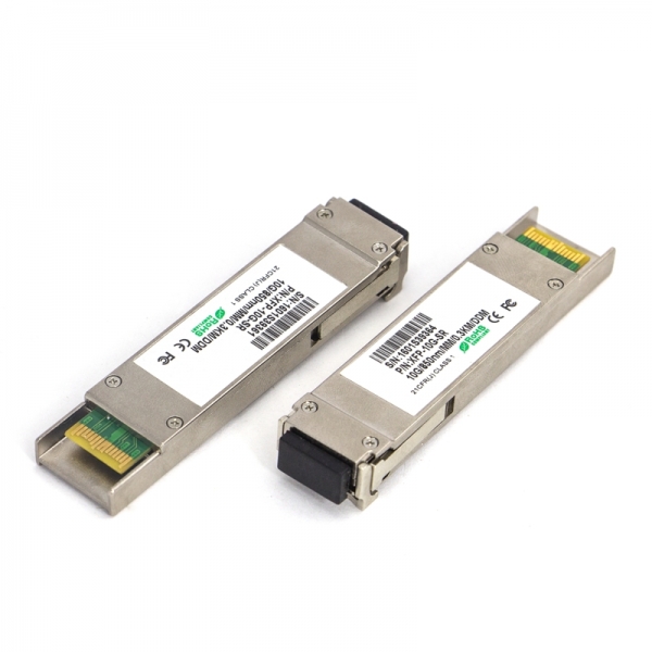
single mode transceiver is small form factor pluggable module for optical data communications such as 10GBASE-LR/LW defined by IEEE 802.3ae. It is with the SFP+ 20-pin connector to allow hot plug capability. The module is designed for single mode fiber and operates at a nominal wavelength of 1270nm or 1330nm; The transmitter section uses a multiple quantum well DFB, which is class 1 laser compliant according to International Safety Standard IEC-60825.The receiver section uses an integrated InGaAs detector preamplifier (IDP) mounted in an optical header and a limiting post-amplifier IC. The transceiver designs are optimized for high perform -ance and cost effective to supply customers the best solutions for telecommunication.
Absolute Maximum Ratings
|
Parameter |
Symbol |
Min. |
Max. |
Unit |
Note |
|
Supply Voltage |
Vcc |
-0.5 |
4.0 |
V |
|
|
Storage Temperature |
TS |
-40 |
85 |
°C |
|
|
Relative Humidity |
RH |
0 |
85 |
% |
|
Note: Stress in excess of the maximum absolute ratings can cause permanent damage to the transceiver.
General Operating Characteristics
|
Parameter |
Symbol |
Min. |
Typ |
Max. |
Unit |
Note |
|
Data Rate |
DR |
9.95 |
|
10.3125 |
Gb/s |
|
|
Supply Voltage |
Vcc |
3.13 |
3.3 |
3.47 |
V |
|
|
Supply Current |
Icc5 |
|
|
300 |
mA |
|
|
Operating Case Temp. |
Tc |
0 |
|
70 |
°C |
|
|
TI |
-20 |
|
80 |
|
Electrical Characteristics (TOP(C) = 0 to 70 ℃, TOP(I) =-20 to 80 ℃,VCC = 3.13 to 3.47 V)
|
Parameter |
Symbol |
Min. |
Typ |
Max. |
Unit |
Note |
|
Differential data input swing |
VIN,PP |
180 |
|
700 |
mVpp |
1 |
|
Transmit Disable Voltage |
VD |
VCC-0.8 |
|
Vcc |
V |
|
|
VEN |
Vee |
|
Vee+0.8 |
|||
|
Input differential impedance |
Rin |
|
100 |
|
Ω |
|
|
Differential data output swing |
Vout,pp |
300 |
|
850 |
mVpp |
2 |
|
Output rise time and fall time |
Tr, Tf |
28 |
|
|
Ps |
3 |
|
LOS asserted |
VLOS_F |
VCC-0.8 |
|
Vcc |
V |
4 |
|
LOS de-asserted |
VLOS_N |
Vee |
|
Vee+0.8 |
V |
4 |
Notes:
1. Connected directly to TX data input pins. AC coupling from pins into laser driver IC.
2. Into 100Ω differential termination.
3. 20 – 80%. Measured with Module Compliance Test Board and OMA test pattern. Use of four 1’s and four 0’s sequence in the PRBS 9 is an acceptable alternative.
4. LOS is an open collector output. Should be pulled up with 4.7kΩ – 10kΩ on the host board. Normal operation is logic 0; loss of signal is logic 1.
Optical Characteristics (TOP(C) = 0 to 70 ℃, TOP(I) =-20 to 80 ℃,VCC = 3.13 to 3.47 V)
|
Parameter |
Symbol |
Min. |
Typ |
Max. |
Unit |
Note |
|
Transmitter |
||||||
|
Operating Wavelength |
λ |
1260 |
1270 |
1280 |
nm |
|
|
1320 |
1330 |
1340 |
|
|||
|
Ave. output power (Enabled) |
PAVE |
-3 |
|
+3 |
dBm |
1 |
|
Side-Mode Suppression Ratio |
SMSR |
30 |
|
|
dB |
|
|
Extinction Ratio |
ER |
4.5 |
|
|
dB |
|
|
RMS spectral width |
Δλ |
|
|
1 |
nm |
|
|
Rise/Fall time (20%~80%) |
Tr/Tf |
|
|
50 |
ps |
|
|
Dispersion penalty |
TDP |
|
|
3.2 |
dB |
|
|
Relative Intensity Noise |
RIN |
|
|
-128 |
dB/Hz |
|
|
Output Optical Eye |
Compliant with IEEE 0802.3ae |
|||||
|
Receiver |
||||||
|
Operating Wavelength |
λ |
1320 |
1330 |
1340 |
nm |
|
|
1260 |
1270 |
1280 |
|
|||
|
Receiver Sensitivity(ER=4.5) |
PSEN1 |
|
|
-12.6 |
dBm |
2 |
|
Receiver Sensitivity(ER=6) |
PSEN2 |
|
|
-14.4 |
2 |
|
|
Average Receive Power |
PAVE |
|
|
0.5 |
dBm |
|
|
Receiver Reflectance |
Rrx |
|
|
-12 |
dB |
|
|
LOS Assert |
Pa |
-30 |
|
|
dBm |
|
|
LOS De-assert |
Pd |
|
|
-17 |
dBm |
|
|
LOS Hysteresis |
Pd-Pa |
0.5 |
|
|
dB |
|
Notes:
1. Average power figures are informative only, per IEEE 802.3ae.
2. Measured with worst ER; BER<10-12; 231 – 1 PRBS.
|
Pin |
Symbol |
Name/Description |
|
1 |
VEET [1] |
Transmitter Ground |
|
2 |
Tx_FAULT [2] |
Transmitter Fault |
|
3 |
Tx_DIS [3] |
Transmitter Disable. Laser output disabled on high or open |
|
4 |
SDA [2] |
2-wire Serial Interface Data Line |
|
5 |
SCL [2] |
2-wire Serial Interface Clock Line |
|
6 |
MOD_ABS [4] |
Module Absent. Grounded within the module |
|
7 |
RS0 |
Rate Select 0 |
|
8 |
RX_LOS [2] |
Loss of Signal indication. Logic 0 indicates normal operation |
|
9 |
RS1 [5] |
Rate Select 1 |
|
10 |
VEER [1] |
Receiver Ground |
|
11 |
VEER [1] |
Receiver Ground |
|
12 |
RD- |
Receiver Inverted DATA out. AC Coupled |
|
13 |
RD+ |
Receiver DATA out. AC Coupled |
|
14 |
VEER [1] |
Receiver Ground |
|
15 |
VCCR |
Receiver Power Supply |
|
16 |
VCCT |
Transmitter Power Supply |
|
17 |
VEET [1] |
Transmitter Ground |
|
18 |
TD+ |
Transmitter DATA in. AC Coupled |
|
19 |
TD- |
Transmitter Inverted DATA in. AC Coupled |
|
20 |
VEET [1] |
Transmitter Ground |
Notes:
1.Module circuit ground is isolated from module chassis ground within the module.
2.should be pulled up with 4.7k – 10k ohms on host board to a voltage between 3.15Vand 3.6V.
3.Tx_Disable is an input contact with a 4.7 kΩ to 10 kΩ pullup to VccT inside the module.
4.Mod_ABS is connected to VeeT or VeeR in the SFP+ module. The host may pull this contact up to Vcc_Host with a resistor in the range 4.7 kΩ to10 kΩ.Mod_ABS is asserted “High” when the SFP+ module is physically absent from a host slot.
Serial Interface for ID and Digital Diagnostic Monitor
The transceiver support the 2-wire serial communication protocol as defined in the SFP+ MSA. The standard SFP+ serial ID provides access to identification information that describes the transceiver’s capabilities, standard interfaces, manufacturer, and other information. Additionally, This SFP+ transceivers provide an enhanced digital diagnostic monitoring interface, which allows real-time access to device operating parameters such as transceiver temperature, laser bias current, transmitted optical power, received optical power and transceiver supply voltage. It also defines a sophisticated system of alarm and warning flags, which alerts end-users when particular operating parameters are outside of a factory set normal range.
The SFP MSA defines a 256-byte memory map in EEPROM that is accessible over a 2-wire serial interface at the 8 bit address 1010000X(A0h), so the originally monitoring interface makes use of the 8 bit address(A2h), so the originally defined serial ID memory map remains unchanged. The structure of the memory map is shown in Table1.
Digital Diagnostic Specifications
The transceivers can be used in host systems that require either internally or externally calibrated digital diagnostics.
|
Parameter |
Symbol |
Units |
Min. |
Max. |
Accuracy |
Note |
|
Transceiver temperature |
DTemp-E |
ºC |
-45 |
+90 |
±5ºC |
1,2 |
|
Transceiver supply voltage |
DVoltage |
V |
2.8 |
4.0 |
±3% |
|
|
Transmitter bias current |
DBias |
mA |
0 |
127 |
±10% |
3 |
|
Transmitter output power |
DTx-Power |
dBm |
-5 |
+5 |
±2dB |
|
|
Receiver average input power |
DRx-Power |
dBm |
-20 |
+1 |
±2dB |
|
Notes:
1.When Operating temp.=0~70 ºC,the range will be min=-5,Max=+75
2. Internally measured
3. The accuracy of the Tx bias current is 10% of the actual current from the laser driver to the laser
Note:
Inductors with DC resistance of less than 1Ω should be used in order to maintain the required voltage at the SFP input pin with 3.3V supply voltage. When the recommended supply filtering network is used, hot plugging of the SFP transceiver module will result in an inrush current of no more than 30 mA greater than the steady state value
Ordering Information
|
Description |
|
SFP+Bidi,9.95 to 10.3Gb/s, 1270/1330nm, 20km, 0~70℃, with Digital Diagnostic Monitor |
|
SFP+Bidi,9.95 to 10.3Gb/s, 1330/1270nm, 20km, 0~70℃, with Digital Diagnostic Monitor |
|
SFP+Bidi,9.95 to 10.3Gb/s, 1270/1330nm, 20km, -20~80℃, with Digital Diagnostic Monitor |
|
SFP+Bidi,9.95 to 10.3Gb/s, 1330/1270nm, 20km, -20~80℃, with Digital Diagnostic Monitor |


 Josie
Josie  Chat Now
 Josie
Josie  Josie
Josie